半岛·游戏官网成立于1995年,总部位于中国安徽阜阳市,是一家专注于体育新闻报道与体育赛事资讯的媒体公司。公司的使命是通过全面深入的报道,为广大体育爱好者提供及时、准确、有深度的体育新闻信息,让人们更深入地了解体育赛事、运动员和体育产业。
作为一家致力于体育新闻报道的专业机构,半岛·游戏官网拥有一支充满激情和专业素养的编辑团队,他们热爱体育,具有丰富的报道经验和深厚的体育知识。公司的报道涵盖了各类体育赛事,包括足球、篮球、网球、田径、游泳等,致力于为读者呈现全方位、多角度的体育新闻。
除了体育新闻报道,半岛·游戏官网还积极参与体育赛事的组织与推广工作。公司与国内外众多体育赛事组织和体育相关机构建立了良好的合作关系,为体育赛事的成功举办提供了全方位的支持与服务。
此外,半岛·游戏官网还致力于推动体育产业的发展,通过组织体育活动、举办体育论坛等方式,促进体育事业的繁荣与发展,为广大体育爱好者创造更多的体育交流与参与机会。
半岛·游戏官网秉承“专业、热情、创新、责任”的价值观,不断完善自身的业务能力,努力成为国内领先的体育新闻媒体公司,为推动体育事业的发展做出更大的贡献。公司将继续秉承“专注体育、服务体育”的宗旨,竭诚为广大体育爱好者提供更优质、更丰富的体育新闻资讯服务。

为体育品牌设计宣传推广策划方案;
为体育赛事和活动定制纪念牌匾;
为体育赛事提供志愿者培训和管理服务。
为体育相关企业提供品牌设计和形象包装服务;
为体育产业投资者提供专业咨询和投资建议;

这家公司的专栏作家都很有见地,每篇文章都很有观点,让人很喜欢看。

这个公司的体育新闻报道非常客观公正,没有夸大事实或者夸张报道,让我感觉很放心!

这个公司的体育资讯服务不仅包括文字报道,还有视频和图片资讯,多种形式满足了我的不同需求!


1.2006年世界杯法国队的所有比赛?2006年德国世界杯小组赛g组日期和时间与游戏次数的对比6月14日00:00法国0-06月19日03:00,法国1-1韩国莱比锡。6月24日03:00多哥0-2法国科隆6月28日星期三03:00西班牙1-3法国1/8决赛汉诺威567月2日星期日3:00巴西0-1法国四分之一决赛法兰克福607月6日半岛·游&#...
1.如何参加2024年全国跆拳道少年锦标赛?参加2024年全国跆拳道少年锦标赛,可以按照以下步骤进行:了解赛事信息:首先,您需要关注中国跆拳道协会或相关机构的官方网站、社交媒体平台或新闻发布,以获取2024年全国跆拳道青少年锦标赛的最新信息。这包括比赛的时间、地点、资格和报名方式。资格:检查资格要求,以确保您符合入职要求。通常,参赛选手需要是一定年龄范围内的青少年,可能需要达到一定的技术水平或训练...

1.谁发明了凉鞋?确切地说,任何鞋类都很难找到指定的发明者,塑料凉鞋也是如此,因为鞋子的生产离不开自然环境和人类智慧。在古代,由于土地崎岖不平,气候严寒酷暑,人类本能地想要保护自己的脚,因此出现了鞋子:简单包裹双脚的兽皮和树叶成为人类历史上最早的鞋子。古人类保存下来的文献仍然可以为我们提供一段精彩的鞋子历史。公元前8000年,在密苏里州发现了美洲土著人的鞋子遗迹。公元前3300年,一位死在法国高山...
1.丹麦世界杯的别称是什么?外号:安徒生童话!我已经有一段时间没有在国际比赛中看到丹麦队了。在错过了2014年世界杯和2016年欧洲杯后,丹麦人依靠球星埃里克森在预选赛第二轮的出色表现获得了第五届世界杯的入场券。在“丹麦童话”年出生的埃里克森的带领下,他们希望用26年的时间书写梦幻般的丹麦童话。绰号“童话王国”,因丹麦童话而闻名。例如,1992年,第九届欧洲足球锦标赛在瑞典举行。由于南斯拉夫的退出...
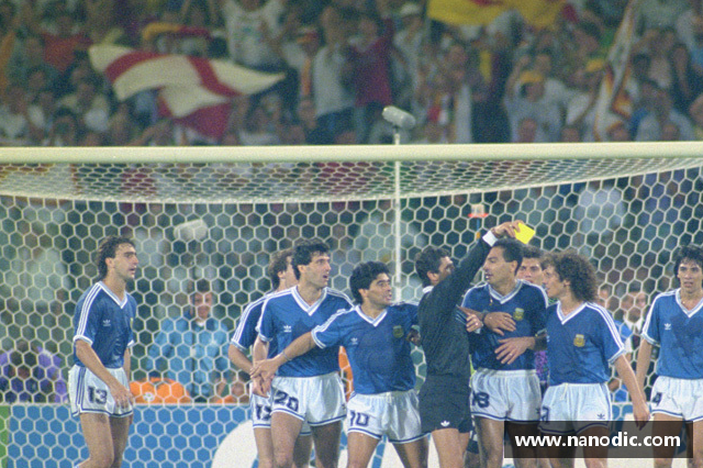
1.1990年世界杯冠军是西德还是德国?1990年世界杯的冠军是德国国家男子足球队。1990年7月8日,在罗马奥林匹克体育场,上一届世界杯的决赛场景再次重演。决赛的双方仍然是联邦德国和阿根廷。然而,此时的阿根廷队已经失去了1986年的辉煌。由于累积的黄牌,四名主力球员无法参加比赛,迭戈·马拉多纳很难独善其身。马特乌斯,布雷默,克林斯曼,沃勒,布赫瓦尔德,利特巴尔斯基,科雷尔和哈西雷是西德队中的伟大...
1.nba第一次出现是几年?NBA每年只有一次选秀大会,选秀顺序会根据各队的赢球情况和抽签结果决定。在选秀大会上,每支球队都有机会选择一名新秀球员,而第一个被选中的球员就是冠军。因此,NBA将在年度选秀中产生一名新的顶级球员。一般来说,虽然每年只有一个冠军,但每年的NBA选秀都是篮球迷非常关注的重大事件,因为这些新秀球员可能会成为未来的篮球巨星。NBA选秀冠军的产生方式是每年会有一次NBA选秀。每...
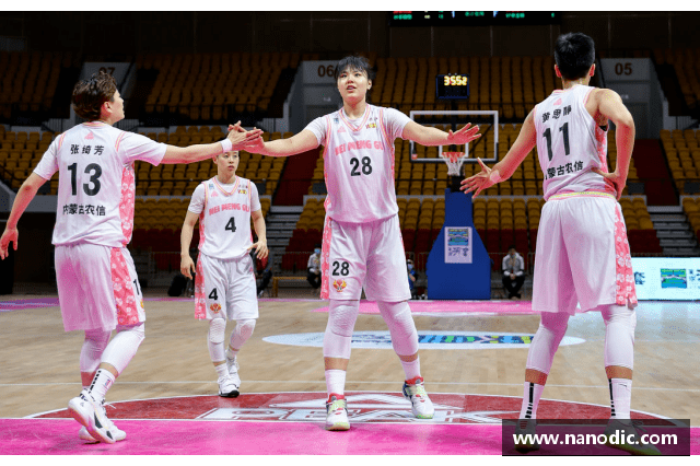
1.2020wcba锦标赛?内蒙古连克新疆获得WCBA冠军!1月3日,在安徽蚌埠进行的2020-2021赛季中国女子篮球联赛(WCBA)总决赛第二场比赛中,内蒙古农信社队以93比82战胜新疆体彩队,以总比分2比0夺得本赛季联赛冠军。在WCBA总决赛第二场比赛中,常规赛冠军、夺冠呼声很高的内蒙古农村信用社1-0领先,再次对阵新疆女篮。尽管这场比赛有点艰难,但内蒙古队以93-82击败了新疆女篮,从而以...
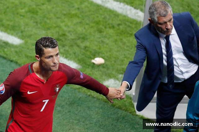
1.葡萄牙人在18年世界杯上的成就?2018年世界杯,葡萄牙1胜2平积5分,以小组第二的成绩晋级淘汰赛。1/4决赛,葡萄牙1-2不敌乌拉圭,止步16强。2018年国际足联世界杯是第21届国际足联世界杯,于2018年6月14日至7月15日举行,为期32天,共有12个体育场。这是世界杯历史上第一次在俄罗斯举行,也是时隔一年。2006年德国世界杯后,它再次回到欧洲。最终的四强是法国、克罗地亚、比利时和英...
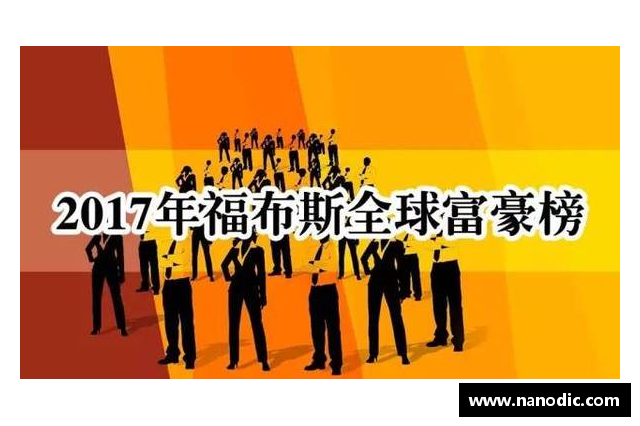
1.福布斯2021浙江富豪榜?第十名,吴光正和鲍培荣。财富(亿元):840亿元;财富增长了19%。公开资料显示,吴光正于1946年9月5日出生于上海。祖籍浙江宁波慈溪,现居中国香港。他是已故船王包玉刚的第二个女婿,也是九龙仓集团的前董事长。2021年3月2日,吴光正和鲍培荣以840亿元人民币的财富位列2021年胡润全球富豪榜第185位。财富增长了19%。第九名,余财富(亿元):900亿元;财富增长...
1.河南体育中心能容纳多少人?1.河南省体育中心的容量约为6万人。2.河南省体育中心是河南省集体体育场馆之一,建筑面积约4.2万平方米。主体育场可容纳约3.6万人,可见其容量相当可观。3.2016年9月,河南省2017年中考在河南省体育中心举行。同时,为确保考试安全有序,河南省在本次考试中设置了11个考区,严格按照安排进行,充分展示了河南省体育中心具有良好的场馆设施和管理运营能力。河南体育中心可容...
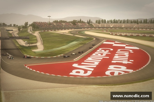
1.方程式赛车水平?方程式赛车是一项汽车竞赛运动,车手使用单座赛车在定制的赛道上进行比赛。目前,世界上有许多级别的方程式赛车,包括:1.一级方程式(Formula One,简称F1):世界最高级别的方程式赛车比赛,世界顶级汽车赛事之一。目前F1赛车使用的发动机是1.6升V6涡轮增压发动机,顶级车队拥有巨大的技术和资金优势。2.公式2(简称F2):F2是F1的下一级。一些年轻车手在F2比赛中获得经验...
1.完整汇集了怀柔旅游景区、八大景区和29个景点。你推荐什么?经过近十年的发展,怀柔的旅游业发展迅速,因为怀柔的山区面积大。形成了各具特色的旅游品牌。下面给大家介绍几条发展最好、规模较大、特色突出的经典经济路线。29个景点:白鹤峡,京北漂流,颜夕湖红螺寺,青龙峡神堂峪,罗红湖度假村,罗红湖鸟岛红螺汇源谷生态风景区慕田峪长城涧口长城(未开发)九股口自然风景区幽谷神潭尤兰原始部落游乐园郊野公园小西湖求...
13594780277
Our Faq
我们会根据市场和服务提供情况适时进行订阅费用的调整,并提前通知用户。
是的,我们提供多种体育赛事的直播服务,用户可以在我们平台上观看直播比赛。
我们公司采取多种安全措施保障用户个人隐私和信息安全,不会泄露用户个人信息,严格遵守相关法律法规。
是的,我们欢迎体育行业相关人士或自媒体向我们投稿,详情请访问我们的投稿页面。